1. 1 Embedded System Introduction
An embedded system is a microcontroller or microprocessor based system which is designed to perform a specific task
1.1. 1.1 Architecture
- Von Neumann: data and code lie in the same memory blocks
- Harvard: data and code lie in different memory blocks
1.2. 1.2 Instruction Set
- CISC: Easy to use, higher clock cycle
- RISC: Hard to use, lower clock cycle
2. 2 8051 Introduction
In 1981, Intel introduced an 8-bit microcontroller called the 8051.
- 128 bytes of RAM
- 4K byte of on-chip ROM
- Max 64K at all because
PCis 16-bit : (0000 to FFFF address) - two timers
- 4 ports (8-bit wide)
- 3 internal and 2 external Interrupts
- Family Member
- 8052: 8K ROM, 256 byte RAM, 3 Timer
- 8031: 0K ROM, 128 byte RAM, 2 Timer
2.1. 2.1 Registers
| Registers | Meaning |
|---|---|
A(8-bit) |
accumulator: quick. Used for all operations |
R(8-bit) |
R0,R1 to R7: store values temporarily |
DPTR(16-bit) |
Data Pointer: access external memory |
PC(16-bit) |
Program Counter: where the next instruction to execute can be found in the memory./starts at 0000h |
SP(8-bit) |
Stack Pointer: the location of the stack’s tail. Initially, the SP register contains value 07 to point to location 08 as the first location being used for the stack by the 8051 |
PSW(8-bit) |
program status word:4 conditional flags + RS0、RS1 |
CY(1-bit) |
there is a carry out from the D7 bit |
AC(1-bit) |
there is a carry from D3 and D4 |
P(1-bit) |
odd number of 1’s in A register, then P = 1 |
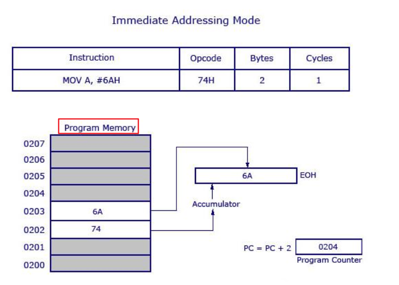
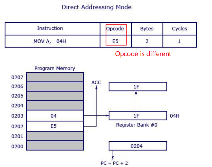
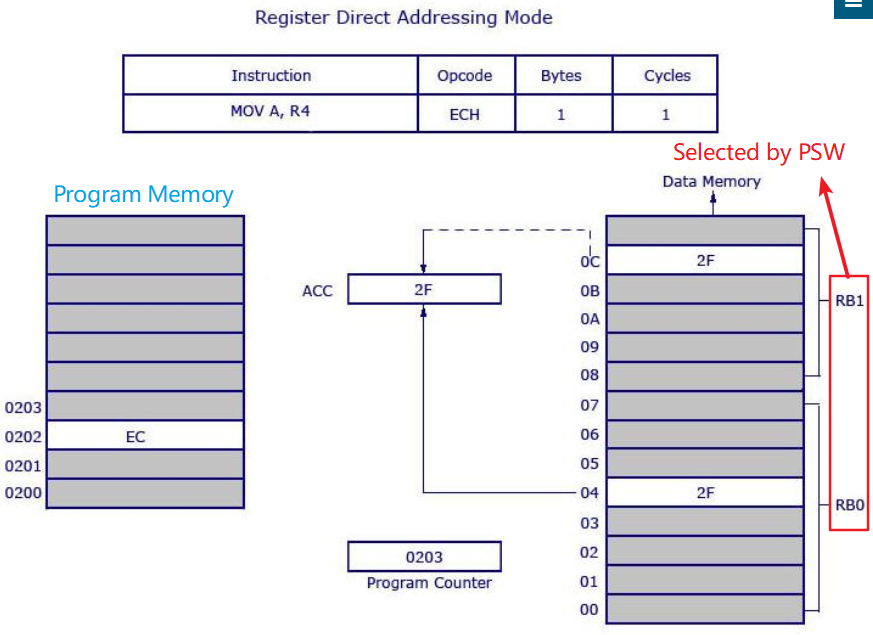
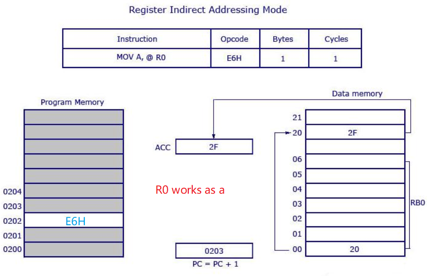
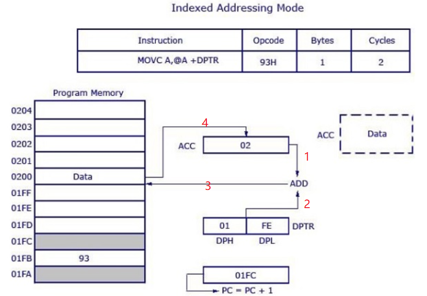
2.2. 2.2 Addressing Modes
- Immediate
- Direct
- Register Direct
- Register Indirect
- Indexed
2.3. 2.3 Hardware
Totally 40 pins
- $4\times8$ ports
- $8$ :
Vcc,GND,XTAL1,XTAL2,EA,ALE,PSEN - default: input. 0 written to a port $\to$ output; 1 written to a port $\to$ input
2.3.1. 2.3.1 Port 0
An open drain:
- we normally connect P0 to 10K-ohm pull-up resistors to use it as an input or output port
- be used as both address and data, designated as AD0-AD7
2.3.2. 2.3.2 Port 1
Can be used either as input or output
- It doesn’t require pull-up resistors because they are already connected internally
2.3.3. 2.3.3 Port 2
Similar to Port 1
- It must be used along with P0 to provide the 16-bit address for the external memory. Port 2 is used for upper 8-bit of the 16 bits address
2.3.4. 2.3.4 Port 3
Similar to Port 1
| P3 Bit | Function |
|---|---|
| P3.0 | RxD |
| P3.1 < | TxD |
| P3.2 < | Complement of INT0 |
| P3.3 < | INT1 |
| P3.4 < | T0 |
| P3.5 < | T1 |
| P3.6 < | WR |
| P3.7 < | Complement of RD |
2.3.5. 2.3.5 Other
RST: Power-On Reset To ensure a valid input of Reset, the high pulse must be high for a minimum of two machine cyclesEA: (External Access) Applying a low pulse, it gets activatedPSEN: (Program store Enable) Applying a low pulse, it gets activatedSingle-Bit Instructions
SETB\CLR\CPL\JB\JNB\JBC
2.4. 2.4 Timers
8051 has 2 timers, Timer 0 and Timer 1
- Both
Timer 0 and 1are 16-bit wide - 2 separate 8-bit registers
TH0\1andTL0\1
2.4.1. 2.4.1 TMOD
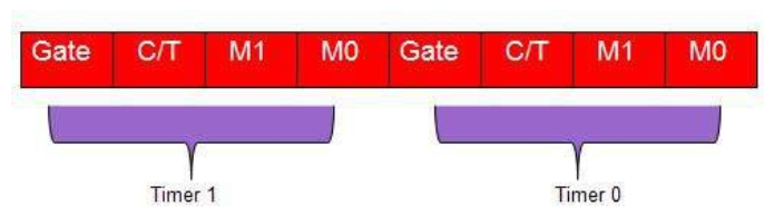
Gate: the timer only runs while INT(0,1) is high. Control the on\off of the timersSoftware: SETB TR0 \ CLR TR0
Hardware:
Gate=1C/T: Counter/Timer select bit.=0: Timers .Be incremented with every machine cycle
=1: Counter
Mode
TF0\1 will be set 1 if Timer has overflowed.
- 0: 13-bit timer mode (8 bits of TH1 and 5 bits of TL1)
- 1: 16-bit timer mode
- 2: 8-bit Auto Reload : Overflow form
TL1setTF1(1) and reloadTL1withTH1
2.5. 2.5 Interrupts
For every interrupt, there must be an interrupt service routine (ISR), or interrupt handler
2.5.1. 2.5.1 Process
- Close currently executing instruction and save the PC in stack
- Jump to memory location of the interrupt vector table and execute ISR
- Get PC from stack, execute from that address
2.5.2. 2.5.2 Priority
We can alter the priority by programming a register called IP (8-bit)(interrupt priority).
default:
| Interrupt | Priority | Meaning |
|---|---|---|
| PT1 | IP.3 | Defines the Timer 1 interrupt priority level. |
| PX1 | IP.2 | Defines the External Interrupt 1 priority level. |
| PT0 | IP.1 | Defines the Timer 0 interrupt priority level. |
| PX0 | IP.0 | Defines the External Interrupt 0 priority level. |
2.5.3. 2.5.3 Enabling
We can enable interrupt by programming a register called IE(8-bit)(interrupt enable).
| EA | - | ET2 | ES | ET1 | EX1 | ET0 | EX0 |
|---|---|---|---|---|---|---|---|
| Global | Undefined | Timer 2 | Serial port | Timer 1 | External 1 | Timer 0 | External 0 |